Eliyan Achieves First Silicon for Breakthrough NuLink PHY Technology
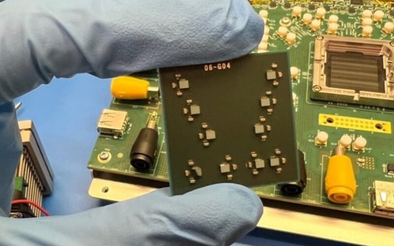


Eliyan, a developer known for its high-performing and efficient chiplet interconnect technology, has announced a significant milestone with the availability of its NuLink PHY technology in silicon. This achievement comes just one year after the company received its initial funding and serves as validation for Eliyan’s UCIe-compatible approach to enabling high-performance and scalable multi-die architectures for compute-intensive applications.
Implemented using TSMC’s standard 5nm process, the NuLink PHY chip operates at an impressive 40Gbps per bump, delivering over 2.2Tbps/mm of beachfront bandwidth at a 130um pitch on standard organic packaging. This performance meets the company’s ambitious power and area targets.
Eliyan’s NuLink PHY technology is highly efficient in terms of area utilization and can deliver up to 3Tbps/mm when implemented on available standard packaging technologies with finer bump pitches, thanks to its innovative interference cancellation techniques.
Industry experts emphasize the economic importance of adopting a chiplet approach in IC design and highlight Eliyan’s chiplet interconnect technology as a compelling solution. John Lorenz, Senior Analyst at Yole Intelligence, predicts a 22% unit growth CAGR in the datacenter GPU hardware market through 2028 and recognizes the potential benefits for chip suppliers in accelerated server computing applications.
Eliyan’s successful silicon implementation demonstrates comparable bandwidth, power efficiency, and latency to die-to-die implementations using advanced packaging technologies but without the complexities and high costs associated with them. The ability to implement chiplet-based systems in standard organic packages opens up possibilities for creating larger system-in-package (SiP) solutions that deliver higher performance per power at lower costs and higher yield.
Ramin Farjadrad, Eliyan’s founding CEO, considers the achievement of first silicon and the obtained results within the set time frame as a significant milestone that establishes them as the leader in efficient chiplet interconnect technology. This milestone positions chip developers to fully leverage the benefits of multi-die architectures without being limited by advanced packaging constraints, enabling the practical mix and match of chiplets across different processes and foundries.
In compute-intensive applications, multi-die architectures are seen as crucial for extensive memory and fast inter-chip communications. Eliyan’s NuLink technology employs novel implementation techniques that significantly differentiate chiplet connectivity in terms of power and performance over any packaging substrate, overcoming supply chain constraints and size limitations associated with traditional interposers.
Eliyan’s chiplet interconnect technology forms the foundation of the Bunch of Wires (BoW) standard, adopted by the Open Compute Project, and is compatible with the UCIe standardization efforts. The company is also collaborating with standards bodies to develop an efficient universal die-to-die interconnect optimized for memory traffic, aiming to accelerate the adoption of memory chiplets.
With silicon characterization data now available, Eliyan is actively working on porting its design to multiple foundry and node technologies based on early customer interest and demand. This progress showcases Eliyan’s commitment to pushing the boundaries of chiplet interconnect technology and meeting the evolving needs of the semiconductor industry.
Researched and Curated by: Anissh Babu